by W.A. Steer PhD
![]()
by W.A. Steer PhD
| Back to contents | About... |
![]()
A "video-digitiser" (also known as a "frame grabber") captures television pictures from a TV set, camera, or video recorder, etc., and forwards them to a computer for display, storage, or general manipulation. This document describes a home-built digitiser which interfaces to an EPP (or bi-directional) parallel port on IBM PCs.
Before embarking on the project, please be sure to realise that this design will not capture movies. At best, it can manage a couple of frames per second. Note also that as described, the circuit collects its picture from a succession of frames. Consequently the image must remain fairly still for the half-second or so taken to capture it. A competent constructor could purchase a larger and more expensive memory chip and modify (simplify) the circuit to overcome the latter limitation if desired (see the Mk.II Video Digitiser).
All video recorders and many TV sets will have a composite video output, usually using a BNC or phono socket. The 21-pin SCART socket found on most domestic AV equipment these days also has a video-out pin.
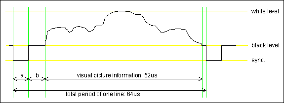
Structure of one video line
In the signal increasing voltage corresponds to increasing brightness. Picture lines are separated by a brief "sync pulse", during which the voltage goes below that of total blackness. Usually the "sync level" is 0V, black level 0.3V, and peak white 1.0V.
In the diagram, region a is the sync, b is the "back porch" (at black level). These are followed by the picture information, finishing with a brief "front porch" (also at black level) before the next line sync. Frames are separated by longer duration sync pulses.
Exact timings are given in the table below.
                   frame  field     line-  back   picture  front   line
            lines   rate   rate      sync  porch     data  porch   total

European     625    25Hz   50Hz     4.7us  5.8us   52.0us  1.5us   64.0us
system

US system    525    30Hz   60Hz     4.7us  4.7us  52.66us  1.5us   63.56us
Note that the "625 lines" means that the line period is 1/625 that of the frame rate. Because the equivalent of several lines is spent in frame syncs, and a further 25 lines at the top of the screen are used to carry teletext information, there are only normally 576 lines of visual data. Some similar decrease will apply to the 525/60 US system.
The broadcast bandwidth is limited to 5-6MHz, giving a maximum horizontal resolution equivalent to about 600 pixels.
Given the above information, in order to capture all the information in a picture it is clearly necessary to digitise the composite video signal at a rate of around 10 million samples per second. Since your average parallel port cannot possibly take data at that rate, some kind of hardware buffer is required - taking data on board at high speed, and releasing it slowly to the computer's port. Modern high-speed First-In First Out (FIFO) memory devices make incredibly simple and convenient buffers.
See block diagram for overall schematic.
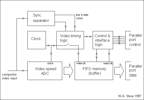
I chose the Bt218KP-20 analog to digital converter because of its high specification and very reasonable price. I could have chosen a 256kb "frame buffer" FIFO, which would permit capture of a whole frame in one go, but for reasons of cost (and because I had other ideas I wanted to experiment with which required only a small buffer), I have used only a 2048byte FIFO, the Am7203A. A natural consequence of using a small buffer is that one picture has to be captured in several goes, spanning about a dozen frames. In the present design "blocks" of 4 scan lines of 512 pixels are captured at a time, then downloaded to the PC. Fast action scenes will inevitably tend to get broken up.
In addition to the ADC and FIFO, a handful of logic gates are required to handle the control and handshaking for the EPP computer interface. Another small section of logic circuitry ensures that we only bother digitising the part of each video signal scan-line which contains useful picture information. Finally a larger module consisting of a binary "scan line" counter and a magnitude comparator is used to govern the collection of "blocks" of 4 scan-lines at a time (and could be omitted if you designed a version with a full-frame FIFO buffer).
All parallel ports have eight "data lines", four output "control" lines,
and five input "status" lines. In the original PC, the standard
parallel port data lines were essentially output-only (ok... there were
hacks!). By a trivial design modification IBM introduced "bi-directional"
data lines on their PS/2 model, where the output-drivers could be software
disabled and data read in using the so-called read-back register.
Unfortunately these didn't generally catch on.
Up to this point all inputs/outputs used TTL signal levels, and timing
and cable specifications were very lax.
Then in the mid nineties, a new range of "enhanced" parallel ports appeared. Basically they tightened up all the electrical specifications, made the data lines bi-directional, and added hardware flow control and data buffering, so that the throughput could be increased dramatically, up to 2MB/sec [though I find 500kB/sec is about the upper limit on my PC, but then it is an old machine with slow bus.]
Enhanced parallel ports come in two flavours of transmission protocol: EPP (enhanced parallel port) which essentially just automates and accelerates the standard handshaking, with extensions for input ability, and ECP (enhanced capability port) which goes a whole stage further with DMA data in/out and scope for hanging multiple devices off one port - making it practically a poor-mans SCSI!
As you might have guessed, implementing ECP in a hardware project would require little short of a microprocessor (or at least LSI chips). For home constructors the EPP-type port provides pretty much all you could want, and is by far the easiest to use.
Most modern PC I/O cards which claim to be "enhanced" or "1284" (see below) will support both protocols, though the settings may be determined by jumpers.
This digitiser circuit requires an EPP type enhanced port.
Parallel ports and especially the enhanced ports are defined in standard IEEE 1284. An excellant abbreviated version of IEEE 1284 is available online at the FAPO web site.
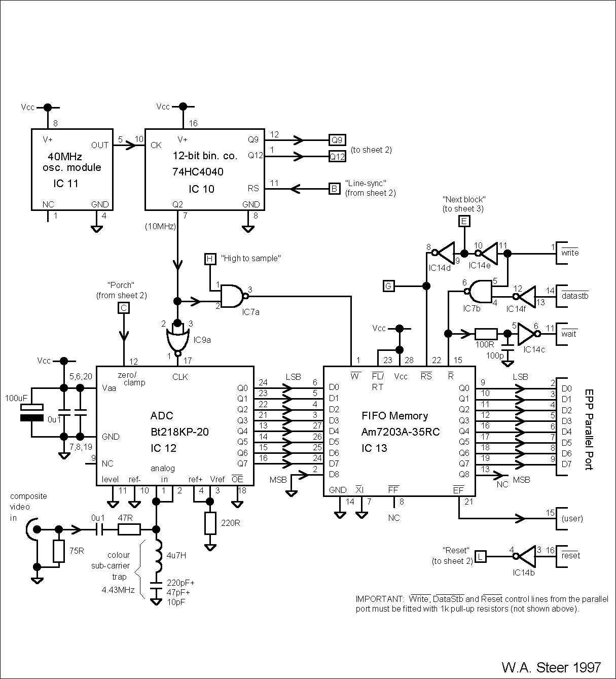
Sheet 2
[Note: Vcc = +5v throughout ]
     IC1        EL4581CN        Video sync-separator
     IC2        74HC14          Hex schmitt inverting buffer
     IC3        74HC4040BE      12-bit binary ripple counter
     IC4        74HC688         8-bit magnitude comparator
     IC5 (no longer required - task now done by IC4)
     IC6        74HC4040        12-bit binary ripple counter
     IC7        74HC00          Quad 2-input NAND gate
     IC8        74HC74          Dual D-latch
     IC9        74HC02          Quad 2-input NOR gate
     IC10       74HC4040        12-bit binary ripple counter
     IC11                       40MHz crystal oscillator module
     IC12       Bt218KP-20      Video-speed ADC
     IC13       Am7203A-35RC    High speed 2048byte 9-bit FIFO buffer
     IC14       74HC14          Hex schmitt inverting buffer
The Bt218KP-20 Video-speed ADC is manufactured by Brooktree, a division
of Rockwell Semiconductor.
The Am7203A-35RC High-speed FIFO buffer is manufactured by Advanced Micro
Devices (AMD), but pin-for-pin equivalents from other suppliers are available.
The EL4581CN video sync separator is made by Elantec, and similar parts are
made by National Semiconductor.
Data sheets for the 74HC logic family are available in PDF format from the
Texas instruments website.
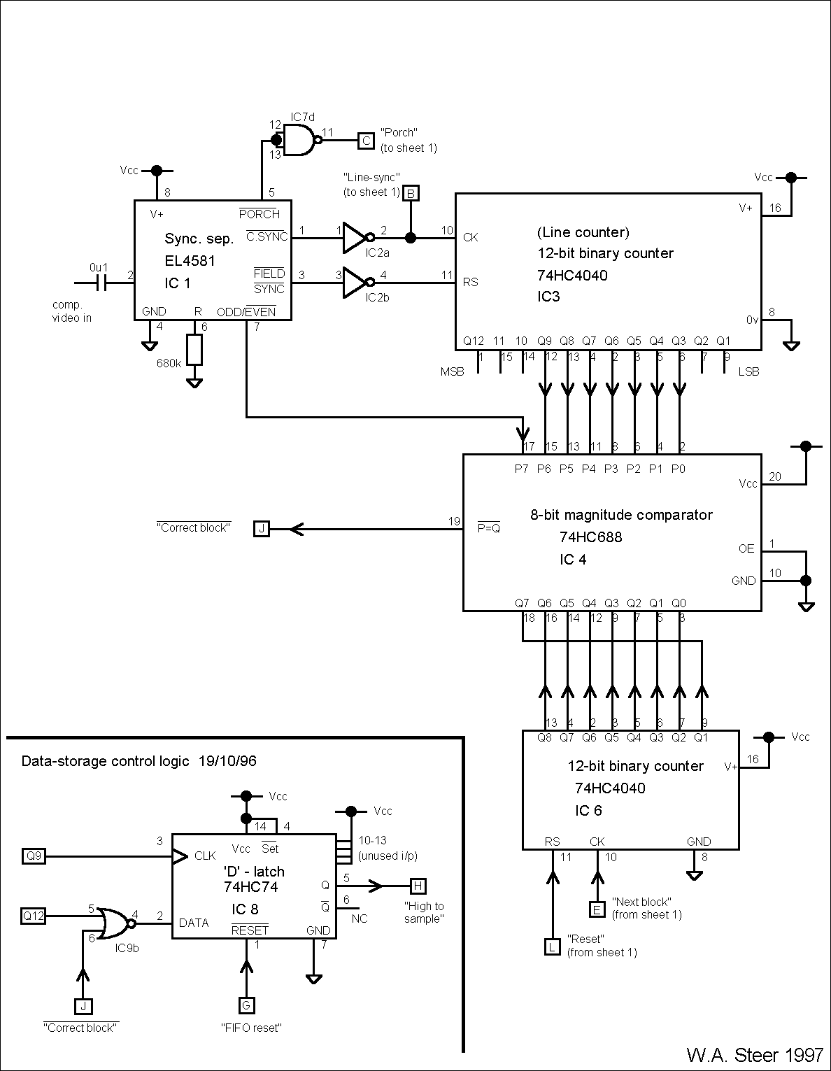
Within each video scan-line we want to ensure that only the useful picture data is stored, and not waste precious space in the FIFO with line syncs and porches. Comparing the video signal with the output of the "master clock divider" binary counter, which is reset during line-syncs, reveals that Q9 goes high at about the times we want data-storage to both commence and cease, with Q12 being low at the start and high at the finish.
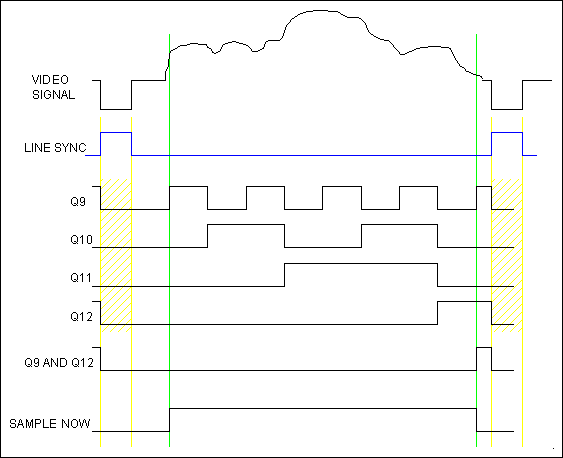
Line timing for data-collection
In the diagram, the trace marked "SAMPLE NOW" shows the signal we would like to derive in order to control the storage of data.
[Sheet 2, inset]
At present, a clean "high to sample" signal is obtained quite elegantly
using a 'D'-latch clocked by Q9 and data input from NOT Q12. [ In reality,
the "correct block" signal (see below) is also brought into the logic
equation at the point where Q12 inverted.]
Given that the method of switching the FIFO write clock using the NAND gate is not inherently synchronous, care is required to ensure we change the state of the control input only while the FIFO clock is HIGH (inactive) that is, when the main clock is LOW. Failure to comply will result in write pulses of sub-standard duration, and possibly jitter on the picture. Since output Q9 of the binary counter changes following the FALLING edge of Q2, the main clock, all should be well. BUT we have to be careful about propagation delays, 8ns typ. for 74HC logic gates, 21ns for the 74HC74 dual D-latch, given that the clock changes state every 50ns! Possibly the biggest problem is that the 74HC4040 is a ripple counter - I ought to (but don't) know how much delay there is between Q2 changing state and Q9 following it!
A further binary counter, IC3, with its clock input connected to the line-sync, and reset to the field-sync, keeps track of the number of the scan line currently being broadcast. Discounting the lower two bits effectively divides the count by four, yeilding the current "block" of 4 lines. Using an 8-bit magnitude comparator, IC4, this is compared to the number of the block "requested" by the software (via counter IC6). In this latest design, the top bit of the comparator compares the field (odd/even) and permits pictures to be captured using the full vertical resolutions. The magnitude comparator gives an high output at J "correct block" when the numbers match.
The real "high to sample" signal is generated by gating the control of our hypothetical "SAMPLE NOW" signal using the "correct block" signal, and completes the organisation of data collection.
Lastly, it is a requirement of the FIFO that both its -Read and -Write clocks must be de-asserted (ie HIGH) during a FIFO reset to guarantee proper operation. This condition has been taken care of in the logic.
[Sheet 1]
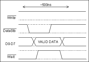
On the output-side of the FIFO, logic taylors the EPP control
signals to meet the requirements of the FIFO read clock.
Essentially, when -Write is HIGH and -DataStb is LOW, the
-ReadClk input of the FIFO is asserted, which causes it to
assert data on its outputs and then increment its internal
read-pointer. At all other times the FIFO outputs are
high-impedance. A slightly retarded (and inverted) copy of the
FIFO -ReadClk provides the EPP -Wait handshake signal. The FIFO
-Empty flag is connected to a user input on the parallel port so
software can test when data becomes available. Software asserts
the EPP -Write signal (making it LOW) to reset the FIFO and
increment the "requested block" counter, and the EPP -Reset
connection is used to reset the "requested block" counter to
zero before commencing a frame-grab. [I may soon replace the
"requested block counter" by an 8-bit latch fed from the
parallel port so that the computer can be in full control of
which lines are collected.]
At one stage I found I had mild vertical streaking on my digitised picture, so it looked a bit like a dodgey photocopy. The problem was fast digital signals getting coupled to the video signal, and the solution was to keep the analog parts away from the digital as far as is reasonably possible, keep leads short, and use a good smothering of decoupling capacitors across the supply rails, particularly next to the clock-divider binary counter. With these precautions my prototype, built on BimBoards, functions perfectly acceptably so requirements don't seem to be too stringent! See the ADC data sheet for more hints on board layout.
All the (DC-level voltage and drive current) interfacing between ICs (ADC, FIFO, control logic...) appear to be within spec., but strictly the FIFO output does not have enough drive current to meet the IEEE 1284 specifications for EPP compatible devices (although it works fine on my particular card). Ideally a buffer IC would be used to interface the EPP data "bus" (and this would also serve to protect the FIFO in the event of a fault, static discharge etc. on the plug).
See my other pages for details of the software interface presented by parallel ports.
Ideally, for fastest performance (particularly if trying to "interlace" blocks - see below) it'd be better to pulse low the -Write line immediately after reading the data, and before doing additional processing so the circuit can be acquiring the next block in the mean time.
If after downloading one block, we wait for the next field and collect the next block then one picture will take 576 lines/4 lines = 144 fields (72 frames), or 2.88 seconds. Hence significant movement in the scene will cause the digitised image to break up somewhat. But we can improve on this: data comes in at 10MHz, and is read out by the computer at approaching 2MHz (on an EPP port) - so the computer will be busy for little over 5 blocks for every one block sampled. From then on, it'd be idly waiting for the next frame to be broadcast. A better idea is to get the circuitry to collect (say) blocks 0,8,16,24,32,... from the first frame, 1,9,17,25,33,... from the next, and 2,10,18,26,34,... etc from the following frame and so on. That way it'll only take a fifth of a second to capture a whole picture (in theory) - a vast improvement. The maximum degree of such interlacing you can manage all depends on the speed of your PC.
With the present hardware it is possible to implement the above scheme by sending multiple "next block" requests to the hardware to get it to retrieve block 8 after block 1, etc., but for a neater and more flexible approach I'd like to try using an 8-bit latch to store the number of the "requested block".
If you need faster throughput and don't mind sacrificing vertical resolution, you could just collect half the vertical lines, and very simply modify the circuit to not care which field it samples.
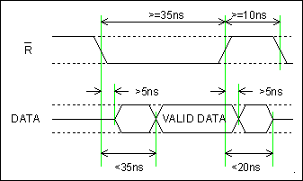
FIFO [Am7203A-35RC] read cycle (source: AMD FIFO data book)
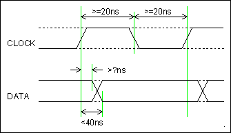
Video ADC [Bt218KP-20] timing (source: Brooktree advance information (data sheet) 8/9/91)
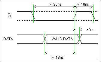
FIFO [Am7203A-35RC] write cycle (source: AMD FIFO data book)

| If you're interested in developing your electronics skills beyond beginner, I can thoroughly recommend
you buy 'The Art of Electronics' by Horowitz and Hill. It's an extremely readable hands-on guide to practical electronics
and packed with real-world experience and know-how. Widely regarded as the 'bible' of electronics...
|
©2001 William Andrew Steer